56G PAM4 NRZ
An ever growing demand of bandwidth of tele and data communication networks continuously requires technological advances and innovations. Today, 100 and 400 Gbps Ethernet interfaces are already commonplace in high-end systems and 800Gbps is coming fast.
Initially separate gearboxes were used for converting, for instance 16 serial NRZ signals to 8 PAM-4 signals and vice versa, but currently silicon vendors such as AMD and Intel have integrated PAM-4 capable transceivers in their devices.
Next to internal studies on how to work with PAM-4 signals and the associated bitrates, AimValley has worked for several customers to design (sub)systems which successfully convey these signals.
Example: development of PCIe plug-in cards which support pluggable optics and/or passive direct attach cables for 400 and 800 Gbps Ethernet with 56 and 112Gbps per lane.


Why PAM-4?
Simply to get more bits per second over a single channel!
By just increasing the frequency, parasitic influences in, for instance the chip’s package, PCB and other interconnects, will increasingly degrade the signal quality. PAM-4 uses 4 discrete signal levels instead of the standard 2 used in NRZ signals, effectively doubling the number of bits transmitted while using virtually the same frequency bandwidth.
From only 2 ‘analog’ levels to 4, doubling the number of bits per symbol.


This doubling of the data rate does not come for free ....
Channel parameters such as insertion loss, return loss and cross-talk all work together to make it increasingly challenging to discriminate between the different signal levels. Due to the closeness of the PAM-4 signal levels, the susceptibility for cross-talk and other external disturbances is about 9.5dB worse than for an NRZ signal.
To make 400G and 800G Ethernet signals more resilient to external disturbances, Gray-coding and Forward Error Correction (FEC) is used.
Gray-code minimizes the binary distance between two adjacent levels within a symbol thus limiting the number of bit errors when a symbol is misread due to noise (up to a certain amount). With only one bit-distance, this results in 1 bit error in the symbol, which is easier to correct by Forward Error Correction (FEC).
AimValley High-Speed Transmission Expertise
Stack-up Definition
The PCB is one of the most important parts of an electronic system. As silicon speeds increase, the PCB must support the higher frequencies as well.
It all starts with a proper stack-up definition.
At AimValley we pay close attention to selecting the right PCB materials such as (ultra-)smooth copper, (ultra-)low loss dielectric materials and when necessary, take into account the glass weave within those materials to avoid skew within a differential pair.
It is good design practice to take special care on how the PCB manufacturer builds-up the PCBs. For example, PCB manufactures may use adhesion promoters which add surface roughness, Or when using microvias, additional copper is grown on top of the already existing layer, which, again, may result in a rougher surface finish.
Proper selection of PCB materials will minimalize losses in the copper and dielectric materials while helping to maintain a characteristic impedance over the entire PCB trace length, and with that minimizing the return loss.
Direct contact with our PCB manufacturers allows us to define PCB stack-ups which focus on selecting the best performing materials and processes while keeping the costs within adequate levels.
Designing for optimal signal integrity
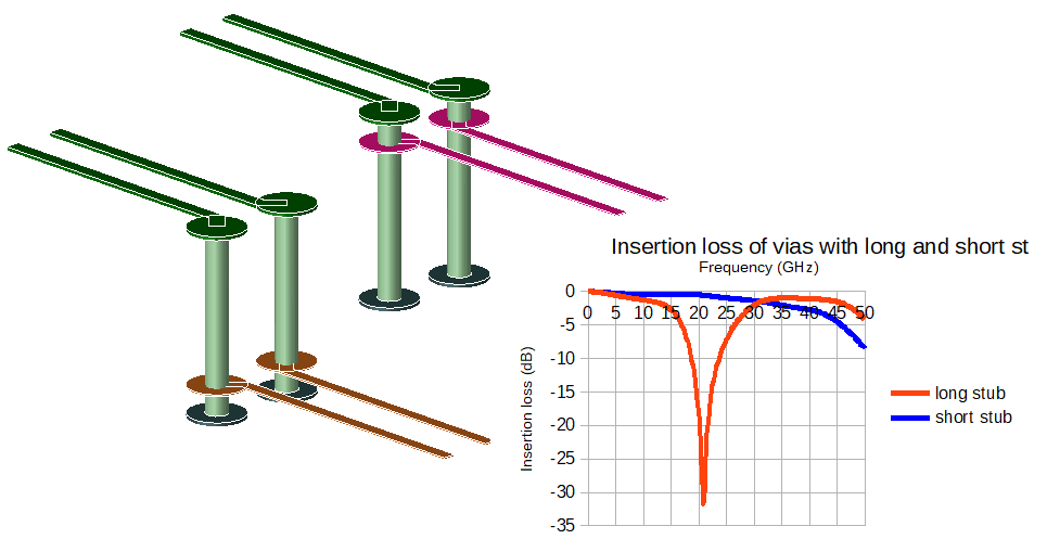
Besides losses in copper, skin-effect and physical trace length between transmitter and receiver, imperfect via design can be a large contributor in losses especially at frequencies above 10GHz.
Using advanced simulation tools, such as Keysight’s Pathwave ADS, we can design and fine-tune the via geometry to minimize the impact on signal integrity.
Just as the via itself, the proximity of stitching vias is of great importance. Without them, the return current through the reference plane(s) will not be following the signal trace itself. This increases the loop area, resulting in improper characteristic impedance of the signal trace/via and increases the risk of EMC and signal integrity issues.
The same tools can also be used to determine the S-parameters which show the cross-talk (both far- and near-end) to see its impact on the signal integrity. If the impact shown is significant, the traces should be moved away from each other.
Via Types and Strategies
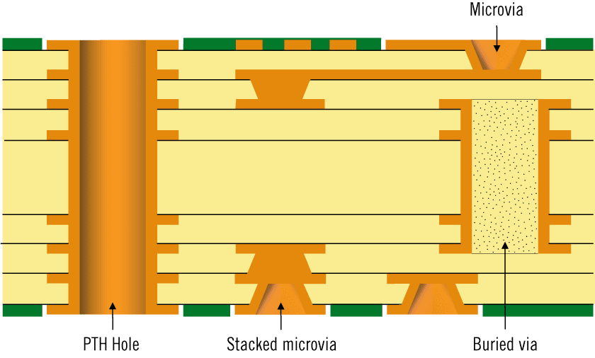
There are multiple types of via (vertical interconnect access) to get a signal from one to another layer. Each via type has its advantages and disadvantages.

The plated thru holes (PTH) is the standard way to connect signals on different layers. Depending on the maximum frequency, the board thickness, substrate materials and on which layers the actual signal traces are located, this may be a good solutions.
However, when not routing on the outer layers of the PCB, this type of via will result in a stub on the transmission line, giving rise to resonances and/or bandwidth limitations, resulting in inter-symbol interference, increasing the deterministic jitter and eye-closure.

Careful layer selection for high-speed signals, can help minimize the stub’s length and keeps your cost down!
Back-drilling the via stub may be a cost effective solution to remove a significant portion of the via stub. Unfortunatley, due to drill depth and PCB pressing tolerances, there will always be a portion left. This residue is usually about 100~200 µm long and can vary between PCB manufacturers.
If frequencies are so high that even the remaining stub proves too much of a disturbance, other via technologies can be used, such as (stacked) micro vias, buried and/or blind vias, all of which result in a stub-less layer change. Careful modeling/simulating is required to get the maximum performance out of the selected method. Since the solution may differ between each chosen stack-up and via strategy, this may be very time consuming. However, it is well worth the effort, bec ause well-designed via structures result in good signal integrity margins, making the overall design more robust.

AimValley proven track record
AimValley has developed a number of (sub-)systems which make use of 400Gbps PAM-4 signaling. The products are used in core telecom infrastructure and range from high-end telecom switching equipment to test and measurement.
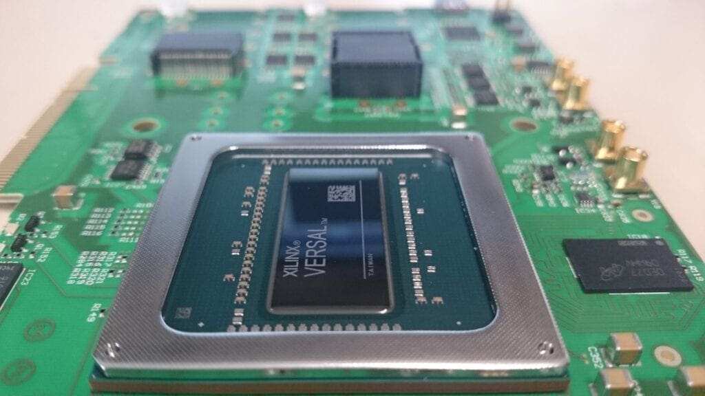
One example is a 400G card for a leading test & measurment company, which adds 400Gbps Ethernet capabilities to their test system.
The front-end of this card is equipped with one QSFP-DD and one QSFP56 connector, both make use of 56Gbps PAM-4 signaling.

