We all know that high-speed product development is a complex business.
There are many challenges to overcome.
Here are some ideas on how AimValley helps you with your next high-speed product design.
- Stack-up definition
- Via types & strategies
- Signal Integrity
Here’s how AimValley tackles these challenges.
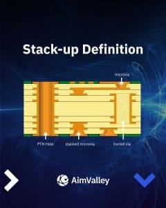
Stack-up definition: the foundation for high-performance PCBs
The PCB is a critical component in any electronic system, especially as silicon speeds continue to rise. To support these higher frequencies effectively, it all starts with a carefully defined PCB stack-up.
At AimValley, we prioritize selecting the right PCB materials, including ultra-low-profile copper, low-loss dielectrics, and, when necessary, the glass weave within these materials to prevent skew in differential pairs. By selecting the appropriate materials, we minimize losses in both copper and dielectric layers, ensuring a stable characteristic impedance across the entire PCB trace length and reducing return loss.
A good design practice goes beyond just material selection. It also requires close collaboration with PCB manufacturers. Thanks to our direct relationships with PCB manufacturers, we can define stack-ups that strike the optimal balance between performance and cost, ensuring the highest quality and reliability in our designs.

Via types & strategies: making the right connection for high-speed designs
In high-speed PCB design, vias (vertical interconnect accesses) are essential for routing signals between layers, but not all vias are created equal. Choosing the right via type can have a significant impact on signal integrity, especially at higher frequencies.
One of the most common via types is the Plated Through-Hole (PTH). This full-depth via can connect all layers of the PCB and is widely used due to its simplicity and cost-effectiveness. Depending on the design requirements, such as board thickness, substrate material, maximum frequency, and which layers carry the signal traces, PTH vias can be a suitable choice.
However, when not routing on the outer layers of the PCB, this type of via results in a stub (unused sections of the via barrel below or above the signal path) on the transmission line. These stubs can act as resonant structures, introducing unwanted reflections and bandwidth limitations. The result? Inter-symbol interference, increased deterministic jitter, and reduced eye diagram opening.
The use of micro vias can eliminate this stub, while back-drilling of the PTH vias removes at least a significant portion, making it suitable for much higher frequencies, albeit at an additional cost and production time.
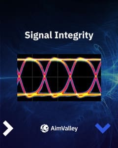
Designing for optimal signal integrity at high frequencies
When designing high-speed circuits, signal integrity is paramount, especially at frequencies above 10GHz. While copper losses, skin effects, and trace length are often discussed, another significant contributor to signal degradation is imperfect via design.
In addition to the via design, the placement of stitching vias plays a crucial role. Without properly placed stitching vias, the return current through the reference plane(s) will not follow the signal trace. This increases loop areas, resulting in less-than-ideal characteristic impedance of the signal trace/via, increasing the potential for EMC issues and signal degradation.
EM Field Simulation tools show trace and via performance. Their detailed results enable us to analyze and optimize via geometries. At AimValley, we use advanced simulation tools like Keysight Technologies’ Pathwave ADS to help fine-tune via geometries to minimize losses and ensure robust signal integrity.
.....And how AimValley helps you to overcome them!

Keeping up with bandwidth demands: designing for 800G and beyond
The relentless growth in bandwidth demand across telecom and data communication networks continues to push the boundaries of technology. While 400G and 800G Ethernet interfaces are already standard in high-performance systems, 1.6Tb/s is rapidly becoming the new benchmark.
Initially, these high-speed connections relied on external gearboxes to convert multiple NRZ lanes into fewer, higher-speed PAM-4 lanes. Today, major silicon vendors like AMD and Intel Corporation have integrated PAM-4 capable transceivers directly into their devices, eliminating the need for separate components and enabling more compact and efficient designs.
At AimValley, we’ve conducted in-depth studies on working with PAM-4 signaling and its higher bitrates. Beyond internal research, we’ve supported multiple customers in designing high-speed (sub)systems that reliably handle these demanding signals.
✅ Example project: Development of PCIe plug-in cards supporting pluggable optics and/or passive direct attach cables for 400Gb/s and 800Gb/s Ethernet, with per-lane data rates of 56Gbps and 112Gbps.
These solutions are a testament to our ability to innovate at the cutting edge of high-speed connectivity.